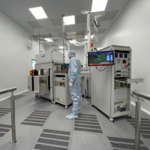
Development history
Development history:
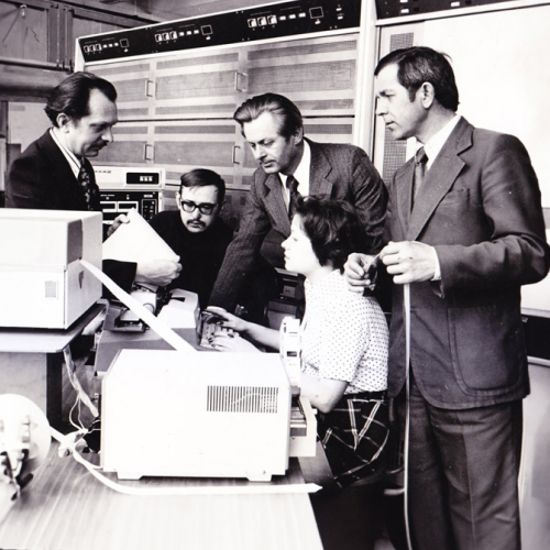
1962-1972
- Research institute establishment and development of film deposition various methods in vacuum.
-
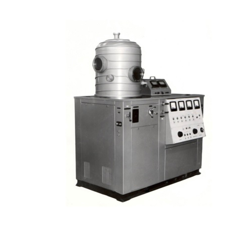
Creation of vacuum equipment with increased productivity by group processing. The first samples of diffusion equipment and industrial equipment for the film layers formation on 60x48 mm glass-ceramic substrates have been developed. Equipment set for the mass production of integrated circuits on 40 and 60 mm silicon wafers have been developed.
1973-1980
- Creation of vacuum equipment with new methods of film deposition and automatic process control (APC), as well as vacuum equipment with loadlock systems.
-
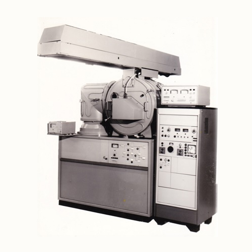
Realization of the magnetron sputtering method for deposition films on Ø 100 mm Si wafers. All necessary types of equipment for the integrated circuits production on 76 mm wafers, including with electron beam and ion systems were developed. The number of the company's employees were awarded the Lenin and State Awards. In the 1960s–1980s, NIITM was virtually the only major developer of vacuum-plasma and physical-thermal equipment in the country.
1981-1989
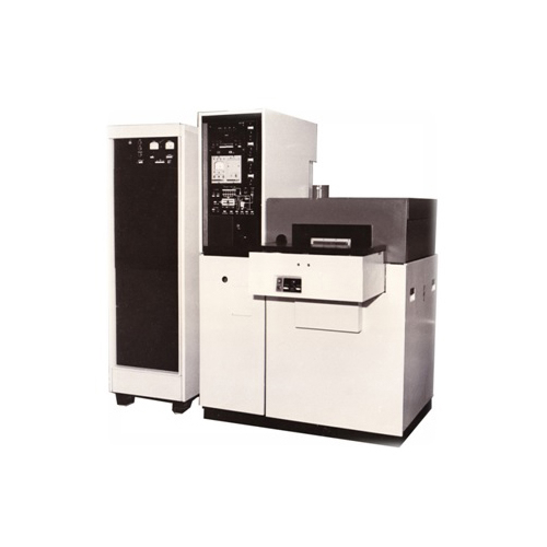
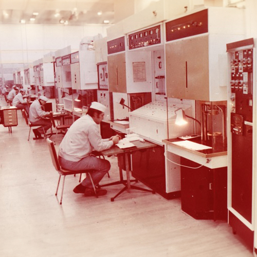
- Creation of high-performance continuous and semi-continuous vacuum equipment with MSU for deposition films on wafers up to Ø 150 mm with loading from cassette to cassette.
-
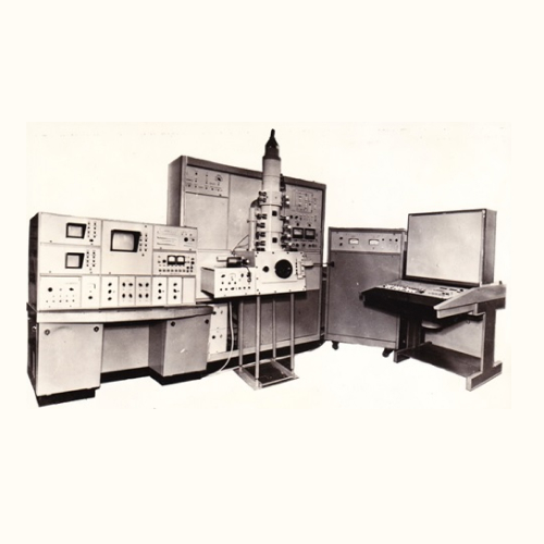
Realization of the oil-free pumping and microprocessor control (MPC). Integration of equipment into a "clean room". The enterprise was awarded the Order of the Red Banner Labor. The Soviet-Bulgarian enterprise "EMKO" was created.
1990-2004
- The restructuring period in the “market” economy conditions.
-
Development of the special cluster technological equipment new generation with technological modules integration in one plant for carrying out micro-cycles. Supply of more than 30 technological plants to China. Scientific directions reduction of institute.
2005-2016
- The stabilization and direction determination period of the research institute’s activities.
-
Creation of the new types semi-continuous and continuous vacuum equipment, as well as cluster systems. Transition to individual Ø 150 mm and Ø 200 mm wafers processing. Development, manufacture and supply set of small-sized vacuum-plasma plants for universities (100-150 mm wafers) for small-scale production; plants for additional purification of ultra-pure hydride gases by low-temperature rectification; the set of plants for additional purification of ultra-pure chloride gases; plant for gas-phase and liquid-phase epitaxial structures growth; cluster equipment for innovative technological processes; vacuum equipment for magnetron films deposition on roll material.
2017-2024
- Participation in Complex Projects and State Programs. Emergence of new activity areas and equipment line expansion.
-
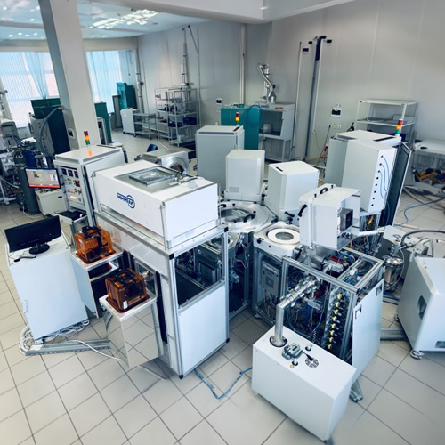
Creation of industrially oriented innovative equipment and cluster complexes based on it for processing Ø 200 and 300 mm wafers. Development, production and supply:
- plants for additional purification of ultra-pure hydride gases by low-temperature rectification;
- a set of plants for additional purification of ultra-pure chloride gases;
- plants for gas-phase and liquid-phase epitaxial growth of structures;
- cluster equipment for innovative technological processes;
- vacuum equipment for magnetron films deposition on roll material;
- ASR implementation (applied scientific research) under the Agreement on the grants provision with the Ministry of Education and Science;
- vacuum system, units and assemblies of a roll-type plant for electronic materials metallization were supplied;
- vacuum-plasma processes complex for 300 mm wafers processing.
- SC NIITM became a co-developer of the Program for the Development of Electronic Engineering until 2030. As part of this program a complex of R & D is being carried out jointly with JSC NIIME: 1) Development of technological modules for critical operations for processing wafers up to 300 mm and a technology level 65 nm (plasma-chemical processes of etching and deposition);
-
2) Creation of domestic equipment for ion implantation.
