+7(495)229-75-01
+7(499)735-13-69 - Marketing department
Contact us
E-mail
marketing@niitm.ru
Address
Zelenograd, Panfilovsky Prospekt, 10
Operating mode
Mon - Thu: 08:30 - 17:30
Fri: 08:30 - 16:15
Contact us
About company
  • About company
  • History
Equipment
  • Classification of equipment
    • Cluster Systems
    • Plasma Chemical Etching (RIE)
    • Chemical Vapour Deposition (СVD)
    • Physical Vapor Deposition (PVD)
    • Epitaxial Structure Growth
    • Gas-Assisted Thermal Processing
  • Cluster equipment
    • CVD
    • PVD
    • RIE
  • New developments
  • Catalog search
Contacts
Zelenograd, Panfilovsky Prospekt, 10
+7(495)229-75-01
+7(499)735-13-69 - Marketing department
Contact us
E-mail
marketing@niitm.ru
Address
Zelenograd, Panfilovsky Prospekt, 10
Operating mode
Mon - Thu: 08:30 - 17:30
Fri: 08:30 - 16:15
About company
  • About company
  • History
Equipment
  • Classification of equipment
    Classification of equipment
    • Cluster Systems
    • Plasma Chemical Etching (RIE)
    • Chemical Vapour Deposition (СVD)
    • Physical Vapor Deposition (PVD)
    • Epitaxial Structure Growth
    • Gas-Assisted Thermal Processing
  • Cluster equipment
    Cluster equipment
    • CVD
    • PVD
    • RIE
  • New developments
    New developments
  • Catalog search
    Catalog search
Contacts
    About company
    • About company
    • History
    Equipment
    • Classification of equipment
      Classification of equipment
      • Cluster Systems
      • Plasma Chemical Etching (RIE)
      • Chemical Vapour Deposition (СVD)
      • Physical Vapor Deposition (PVD)
      • Epitaxial Structure Growth
      • Gas-Assisted Thermal Processing
    • Cluster equipment
      Cluster equipment
      • CVD
      • PVD
      • RIE
    • New developments
      New developments
    • Catalog search
      Catalog search
    Contacts
      +7(499)735-13-69 - Marketing department
      Contact us
      E-mail
      marketing@niitm.ru
      Address
      Zelenograd, Panfilovsky Prospekt, 10
      Operating mode
      Mon - Thu: 08:30 - 17:30
      Fri: 08:30 - 16:15
      Phone
      +7(499)735-13-69 - Marketing department
      Свяжитесь с нами
      • About company
        • About company
        • About company
        • History
      • Equipment
        • Equipment
        • Classification of equipment
          • Classification of equipment
          • Cluster Systems
          • Plasma Chemical Etching (RIE)
          • Chemical Vapour Deposition (СVD)
          • Physical Vapor Deposition (PVD)
          • Epitaxial Structure Growth
          • Gas-Assisted Thermal Processing
        • Cluster equipment
          • Cluster equipment
          • CVD
          • PVD
          • RIE
        • New developments
        • Catalog search
      • Contacts
      Contact us
      • +7(499)735-13-69 Marketing department
        • Phones
        • +7(499)735-13-69 Marketing department
        • Order a call
      • Zelenograd, Panfilovsky Prospekt, 10
      • marketing@niitm.ru
      • Mon - Thu: 08:30 - 17:30
        Fri: 08:30 - 16:15

      Classification of equipment

      Main
      —
      Catalog
      —Classification of equipment
      Cluster Systems
      Cluster Systems
      Plasma Chemical Etching (RIE)
      Plasma Chemical Etching (RIE)
      Chemical Vapour Deposition (СVD)
      Chemical Vapour Deposition (СVD)
      Physical Vapor Deposition (PVD)
      Physical Vapor Deposition (PVD)
      Epitaxial Structure Growth
      Epitaxial Structure Growth
      Gas-Assisted Thermal Processing
      Gas-Assisted Thermal Processing
      Фильтр
      По популярности (убывание)
      По наименованию (А-Я)
      По наименованию (Я-А)
      По популярности (возрастание)
      По популярности (убывание)
      Фильтр
      Wafer diameter
      Показать все
      Show:
      Wafer loading
      Показать все
      Show:
      Выбрано: 0 Показать
      Выбрано: 0
      Wafer diameter
      200mm, 300mm
      Wafer loading
      FOUP container, SMIF container
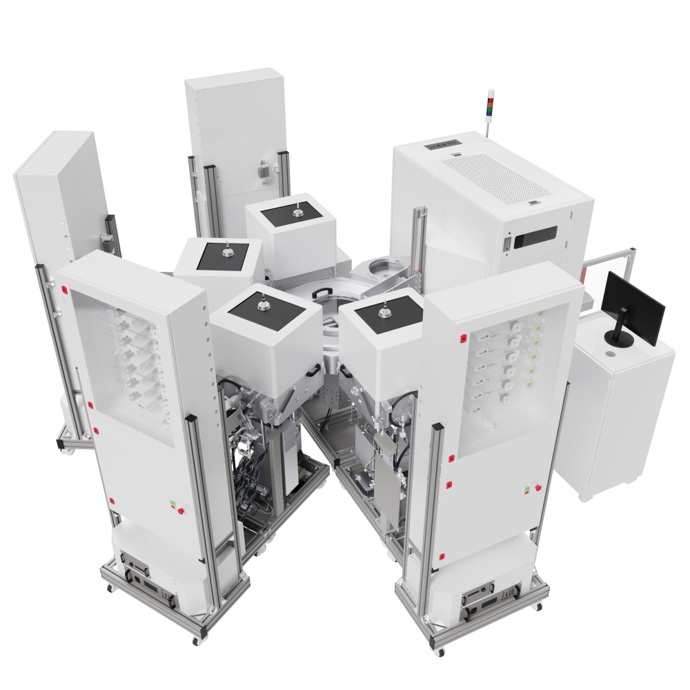
      CLUSTER TM-300 CVD
      CLUSTER TM-300 CVD
      The cluster system is designed for plasma chemical deposition (CVD) with up to 65 nm design rules
      More >
      Wafer diameter
      200mm, 300mm
      Wafer loading
      FOUP container, SMIF container
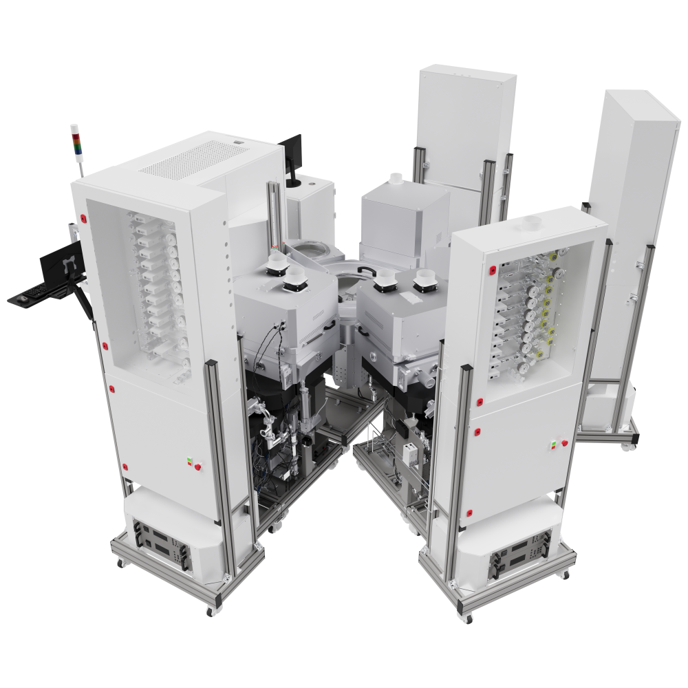
      CLUSTER TM-300 RIE
      CLUSTER TM-300 RIE
      The cluster system is designed for plasma chemical etching (RIE) with up to 65 nm design rules
      More >
      Wafer diameter
      Up to 100mm, 100mm, 150mm, 200mm
      Wafer loading
      From cassette to cassette, Loadlock, SMIF container
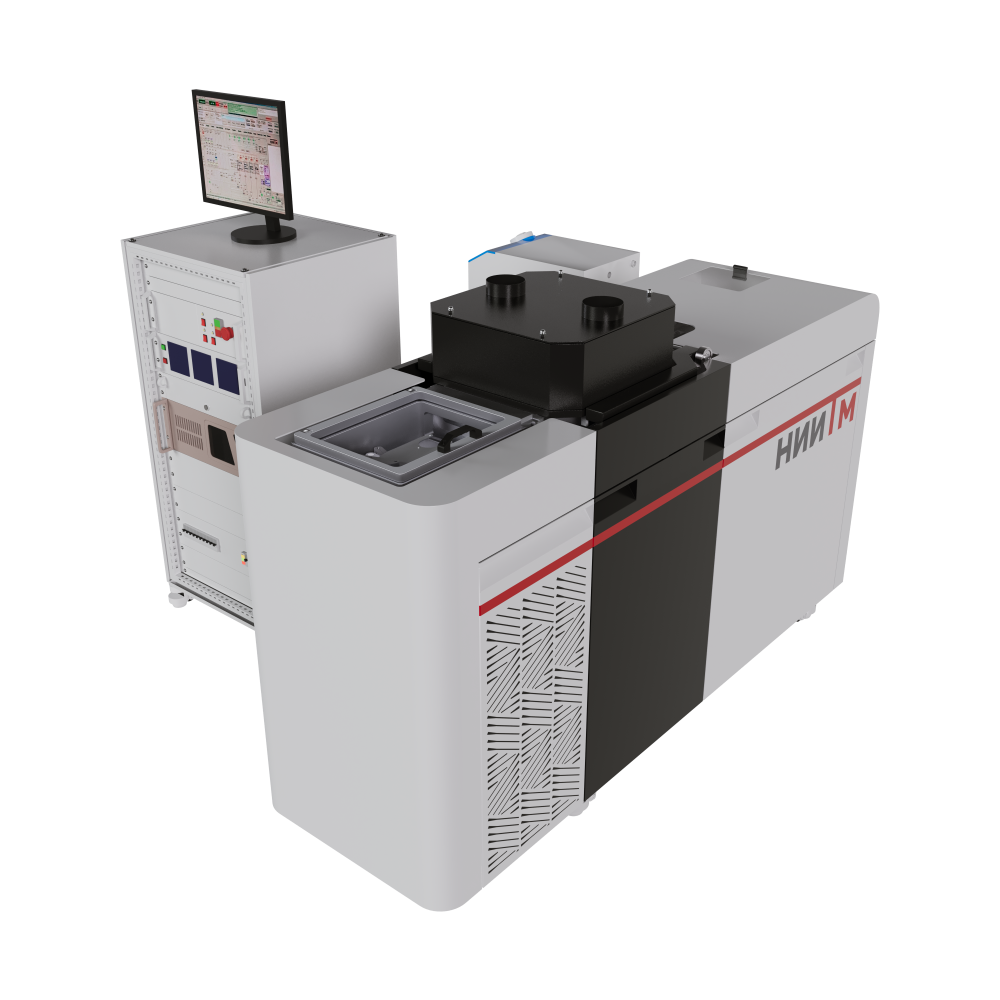
      BTO TM 200-01
      BTO TM 200-01
      Ion-alloyed layers annealing; ohmic contacts formation; metal silicides, thin oxide and dielectric films production; amorphous and polycrystalline films recrystallization, etc.
      More >
      Wafer diameter
      Up to 100mm, 100mm, 150mm, 200mm
      Wafer loading
      From cassette to cassette, Loadlock, SMIF container
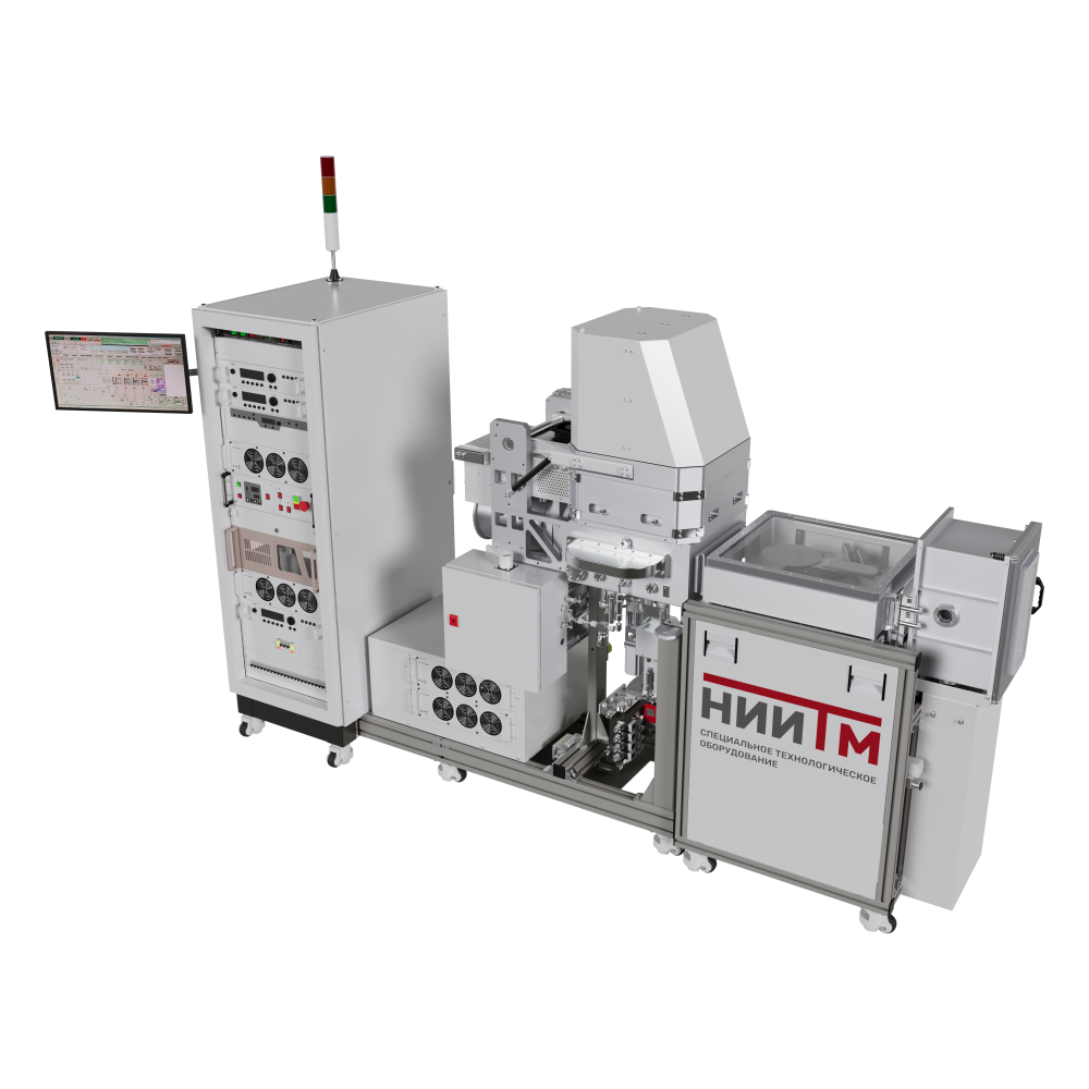
      MAGNA TM 200-04
      MAGNA TM 200-04
      Magnetron sputtering of aluminum (Al) metallization, formation of adhesive, barrier (Ta/TaN, Ti/TiN) and nucleated copper (Cu) layers for bridges in contact and via holes of interlayer joints, etc.
      More >
      Wafer diameter
      Up to 100mm, 100mm, 150mm, 200mm
      Wafer loading
      From cassette to cassette, Loadlock, SMIF container
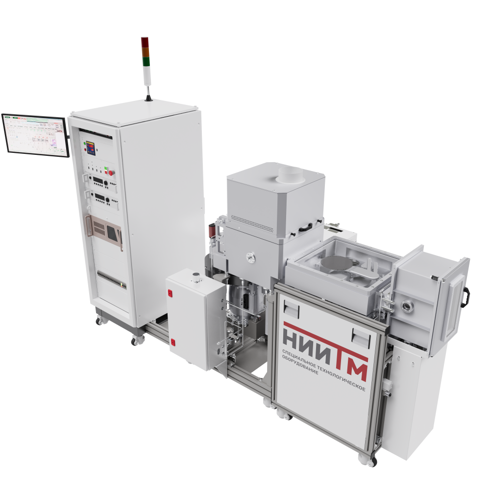
      ISOPHAZ TM 200-02
      ISOPHAZ TM 200-02
      Dielectric layers deposition with an ICP plasma source to form gap and interlayer insulation, including on the contact walls and via holes of interlayer connections
      More >
      Wafer diameter
      Up to 100mm, 100mm, 150mm, 200mm
      Wafer loading
      From cassette to cassette, Loadlock, SMIF container
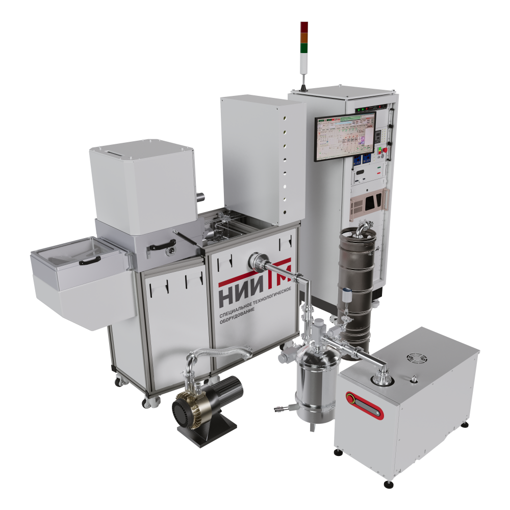
      ISOPHAZ TM 200-01
      ISOPHAZ TM 200-01
      Plasma-enhanced atomic-layer deposition (PEALD)
      More >
      Wafer diameter
      Up to 100mm, 100mm, 150mm, 200mm
      Wafer loading
      From cassette to cassette, Loadlock, SMIF container
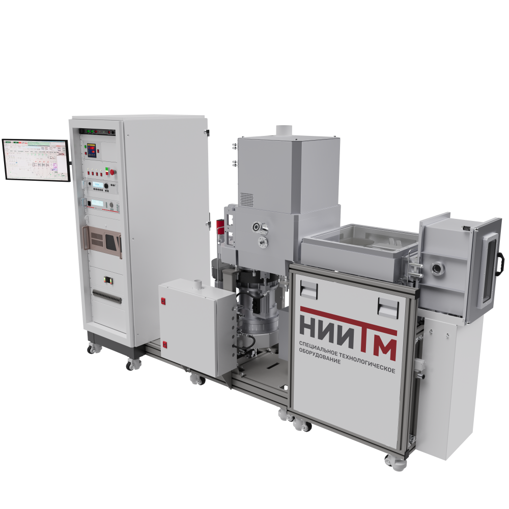
      PLASMA TM 200-04
      PLASMA TM 200-04
      Atomic layer etching of silicon oxide, silicon and surface cleaning
      More >
      Wafer diameter
      Up to 100mm, 100mm, 150mm, 200mm
      Wafer loading
      From cassette to cassette, Loadlock, SMIF container
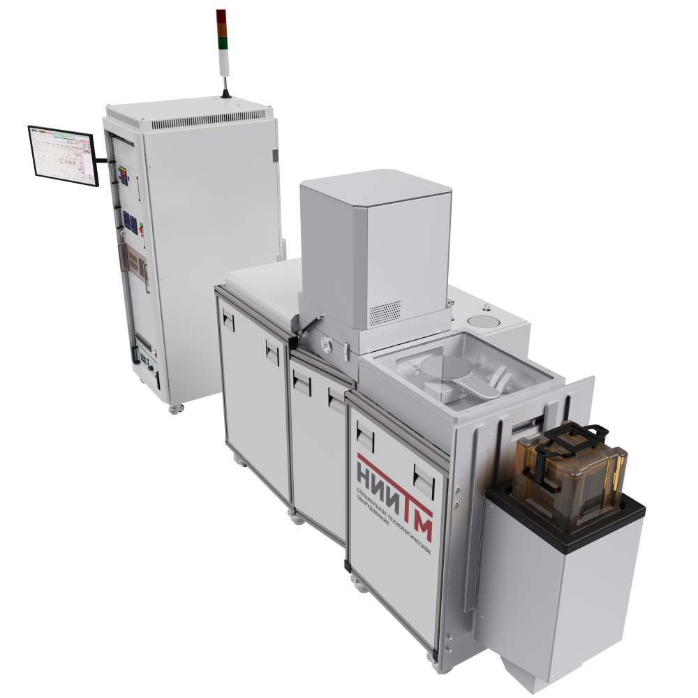
      PLASMA TM 200-03
      PLASMA TM 200-03
      Highly selective processes of photoresist mask plasma-chemical removal and organic polymers etching
      More >
      Wafer diameter
      Up to 100mm, 100mm, 150mm, 200mm
      Wafer loading
      From cassette to cassette, Loadlock, SMIF container
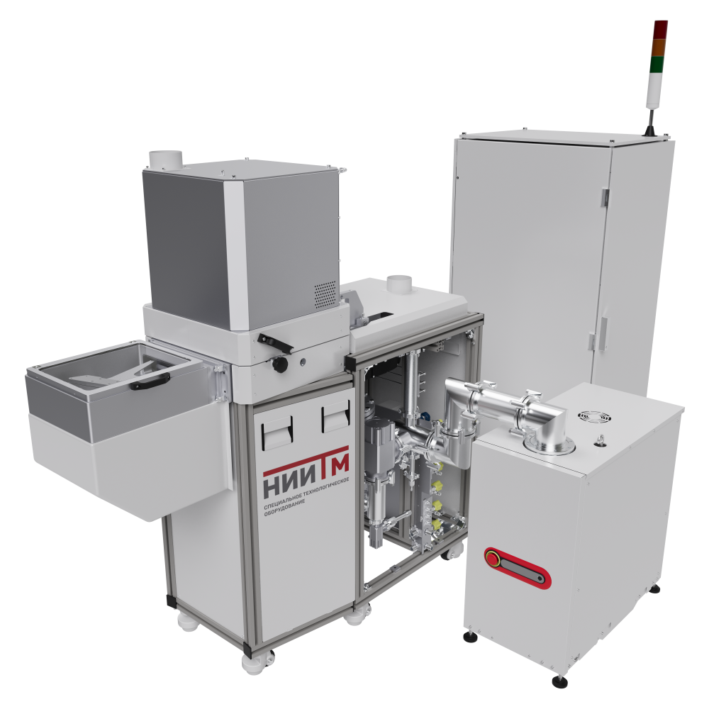
      PLASMA TM 200-02
      PLASMA TM 200-02
      Deep plasma-chemical anisotropic etching of silicon in the MEMS, NEMS, 2.5D and 3D production, as well as through high-aspect holes, etc. based on the Bosch process.
      More >
      Wafer diameter
      Up to 100mm, 100mm, 150mm, 200mm
      Wafer loading
      From cassette to cassette, Loadlock, SMIF container
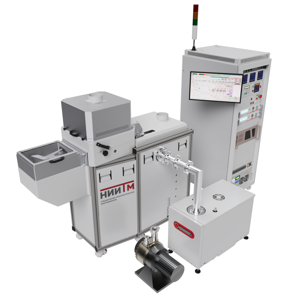
      PLASMA TM 200-01
      PLASMA TM 200-01
      Plasma-chemical etching of polycrystalline silicon and silicon nitride (fine-gap insulation in silicon).
      More >
      Load more
      1 2
      Catalog
      • Classification of equipment
        • Cluster Systems
        • Plasma Chemical Etching (RIE)
        • Chemical Vapour Deposition (СVD)
        • Physical Vapor Deposition (PVD)
        • Epitaxial Structure Growth
        • Gas-Assisted Thermal Processing
      • Cluster equipment
        • CVD
        • PVD
        • RIE
      • New developments
      • Catalog search
      Company
      About company
      History
      Equipment
      Classification of equipment
      Cluster equipment
      New developments
      Catalog search
      Contacts
      +7(495)229-75-01
      +7(499)735-13-69 - Marketing department
      Contact us
      E-mail
      marketing@niitm.ru
      Address
      Zelenograd, Panfilovsky Prospekt, 10
      Operating mode
      Mon - Thu: 08:30 - 17:30
      Fri: 08:30 - 16:15
      marketing@niitm.ru
      Zelenograd, Panfilovsky Prospekt, 10
      © 2026 niitm.ru
      Privacy policy