
Wafer diameter
200mm, 300mm

Wafer loading
FOUP container, SMIF container
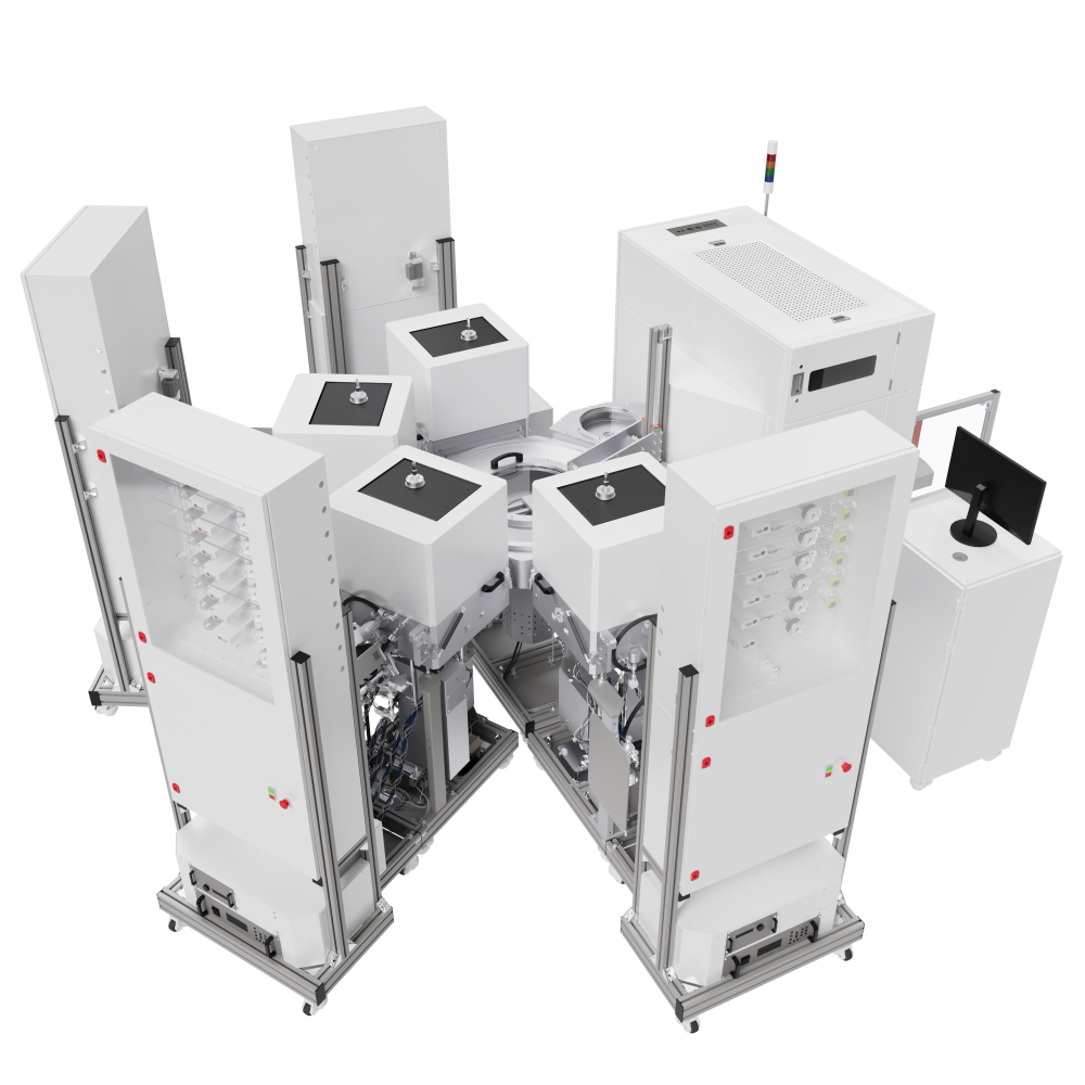
The cluster system is designed for plasma chemical deposition (CVD) with up to 65 nm design rules
Wafer diameter
200mm, 300mm
Wafer loading
FOUP container, SMIF container
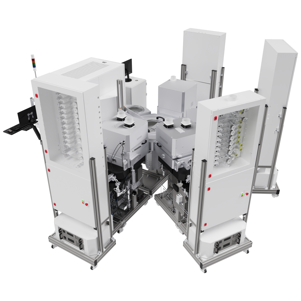
The cluster system is designed for plasma chemical etching (RIE) with up to 65 nm design rules
Wafer diameter
200mm, 300mm
Wafer loading
SMIF container
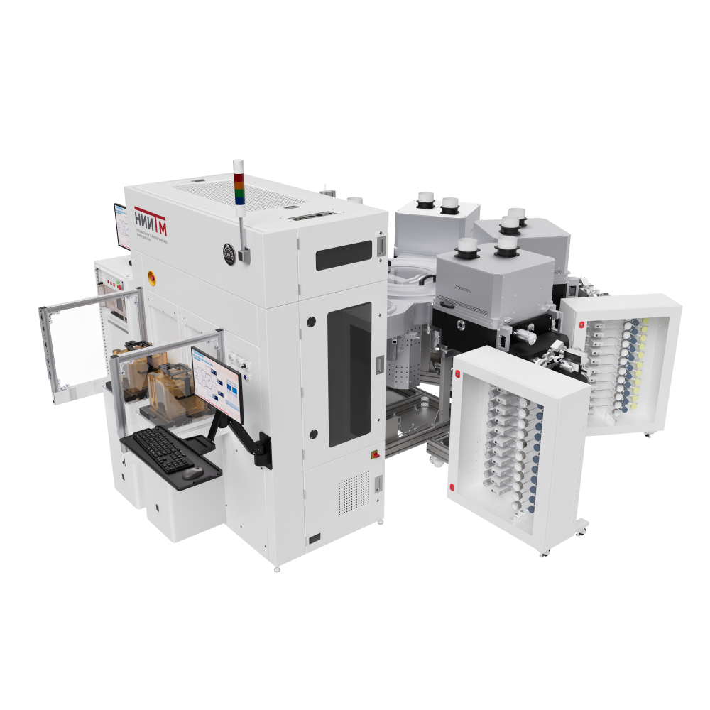
The cluster system is designed to carry out the processes of plasma chemical etching of polysilicon to form circuit elements (gates of various types, slit insulation) by plasma chemical etching of silicon using a photoresistive mask and a rigid mask on functional substrates.
Wafer diameter
200mm, 300mm
Wafer loading
SMIF container
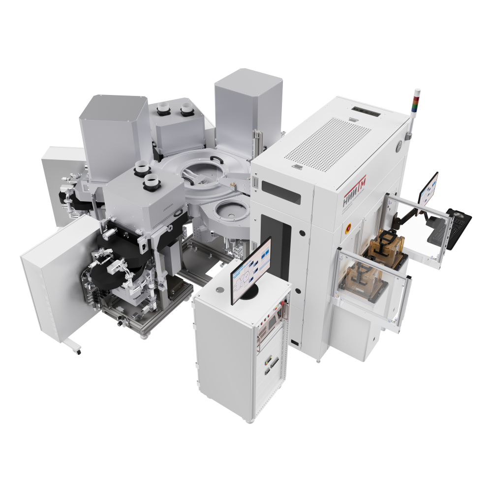
The cluster system is designed to carry out the processes of plasma chemical etching (ICP RIE) of metallization layers for the formation of metal wiring elements by plasma chemical etching of Al (aluminum) using a photoresistive mask on functional substrates.