+7(495)229-75-01
+7(499)735-13-69 - Marketing department
Contact us
E-mail
marketing@niitm.ru
Address
Zelenograd, Panfilovsky Prospekt, 10
Operating mode
Mon - Thu: 08:30 - 17:30
Fri: 08:30 - 16:15
Contact us
About the company
  • About the company
  • Development history
Equipment
  • Classification of equipment
    • Plasma Chemical etching – PCE
    • Plasma chemical deposition – PCD
    • Physical deposition - PVD
    • Growing epitaxial structures
    • Heat treatment
    • Precision cleaning
  • Cluster equipment
    • PCD
    • PCE
    • PVD
  • New developments
  • Catalog search
Contacts
Zelenograd, Panfilovsky Prospekt, 10
+7(495)229-75-01
+7(499)735-13-69 - Marketing department
Contact us
E-mail
marketing@niitm.ru
Address
Zelenograd, Panfilovsky Prospekt, 10
Operating mode
Mon - Thu: 08:30 - 17:30
Fri: 08:30 - 16:15
About the company
  • About the company
  • Development history
Equipment
  • Classification of equipment
    Classification of equipment
    • Plasma Chemical etching – PCE
    • Plasma chemical deposition – PCD
    • Physical deposition - PVD
    • Growing epitaxial structures
    • Heat treatment
    • Precision cleaning
  • Cluster equipment
    Cluster equipment
    • PCD
    • PCE
    • PVD
  • New developments
    New developments
  • Catalog search
    Catalog search
Contacts
    About the company
    • About the company
    • Development history
    Equipment
    • Classification of equipment
      Classification of equipment
      • Plasma Chemical etching – PCE
      • Plasma chemical deposition – PCD
      • Physical deposition - PVD
      • Growing epitaxial structures
      • Heat treatment
      • Precision cleaning
    • Cluster equipment
      Cluster equipment
      • PCD
      • PCE
      • PVD
    • New developments
      New developments
    • Catalog search
      Catalog search
    Contacts
      +7(499)735-13-69 - Marketing department
      Contact us
      E-mail
      marketing@niitm.ru
      Address
      Zelenograd, Panfilovsky Prospekt, 10
      Operating mode
      Mon - Thu: 08:30 - 17:30
      Fri: 08:30 - 16:15
      Phone
      +7(499)735-13-69 - Marketing department
      Свяжитесь с нами
      • About the company
        • About the company
        • About the company
        • Development history
      • Equipment
        • Equipment
        • Classification of equipment
          • Classification of equipment
          • Plasma Chemical etching – PCE
          • Plasma chemical deposition – PCD
          • Physical deposition - PVD
          • Growing epitaxial structures
          • Heat treatment
          • Precision cleaning
        • Cluster equipment
          • Cluster equipment
          • PCD
          • PCE
          • PVD
        • New developments
        • Catalog search
      • Contacts
      Contact us
      • +7(499)735-13-69 Marketing department
        • Phones
        • +7(499)735-13-69 Marketing department
        • Order a call
      • Zelenograd, Panfilovsky Prospekt, 10
      • marketing@niitm.ru
      • Mon - Thu: 08:30 - 17:30
        Fri: 08:30 - 16:15

      Cluster PCE Al

      Main
      —
      Catalog
      —
      New developments
      —Cluster PCE Al
      Cluster PCE Al
      Contact us
      Ask a question
      Additional options are possible
      Cluster PCE Al
      Cluster PCE Al
      Cluster PCE Al
      Cluster PCE Al
      Cluster PCE Al
      Cluster PCE Al
      Cluster PCE Al
      Cluster PCE Al
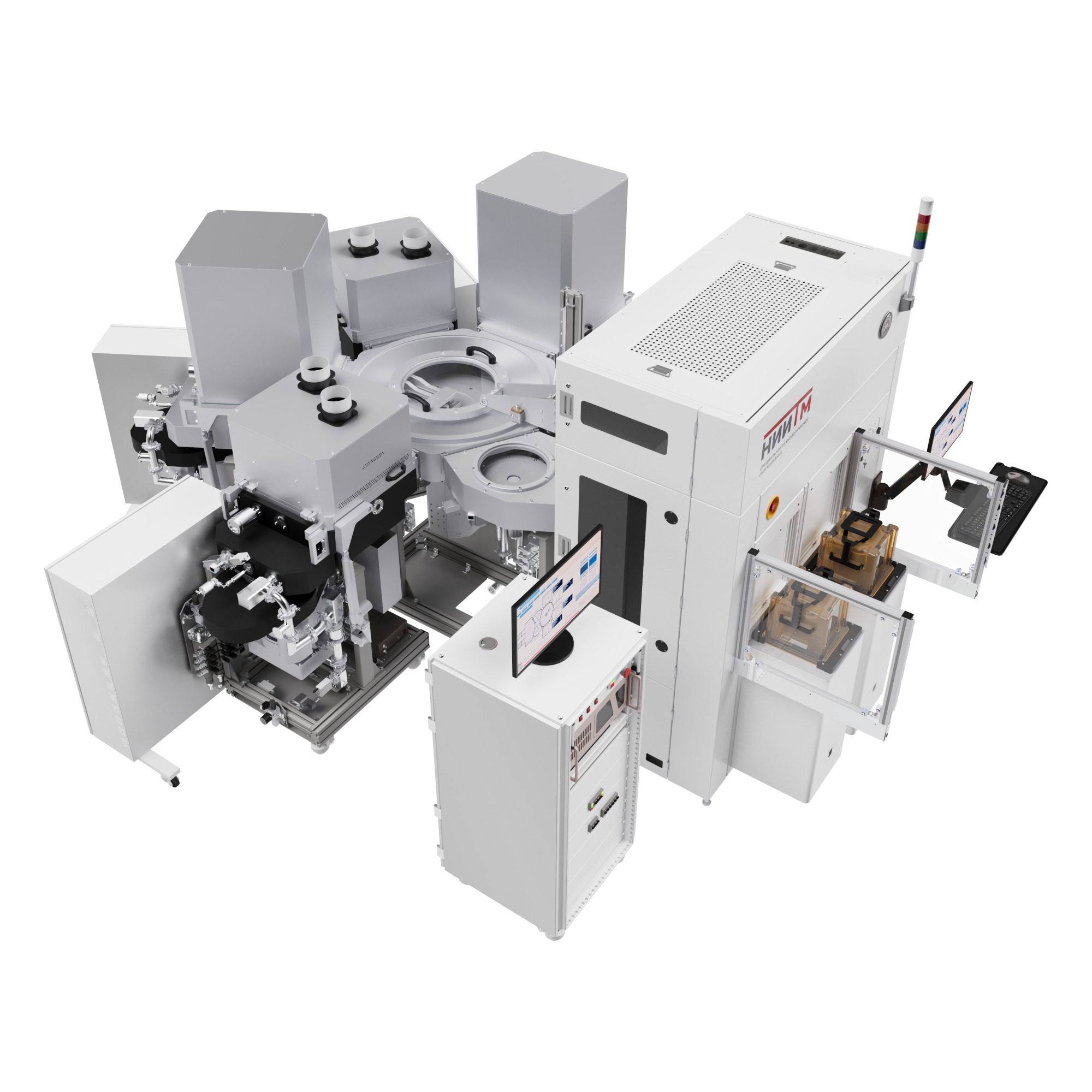
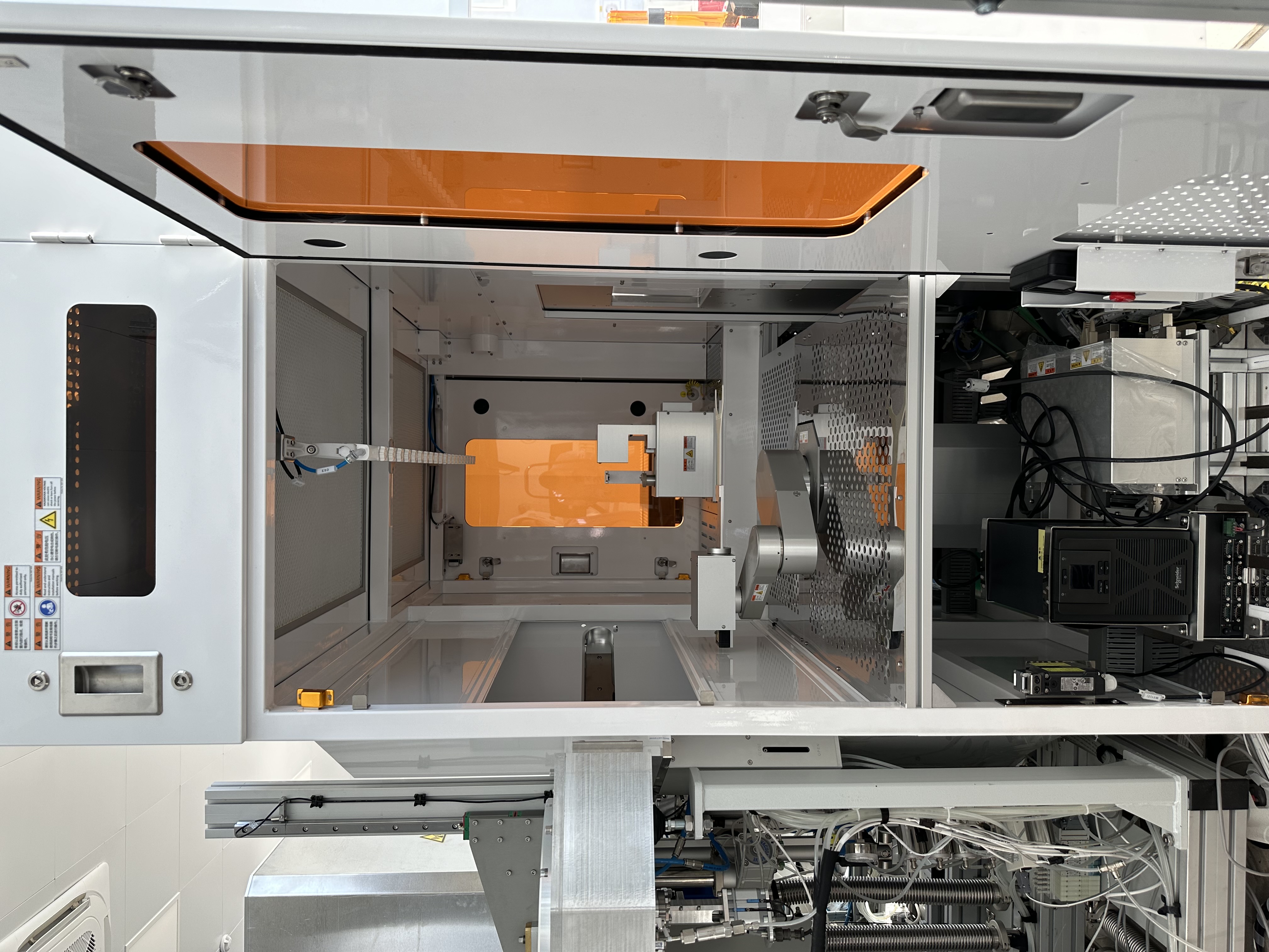
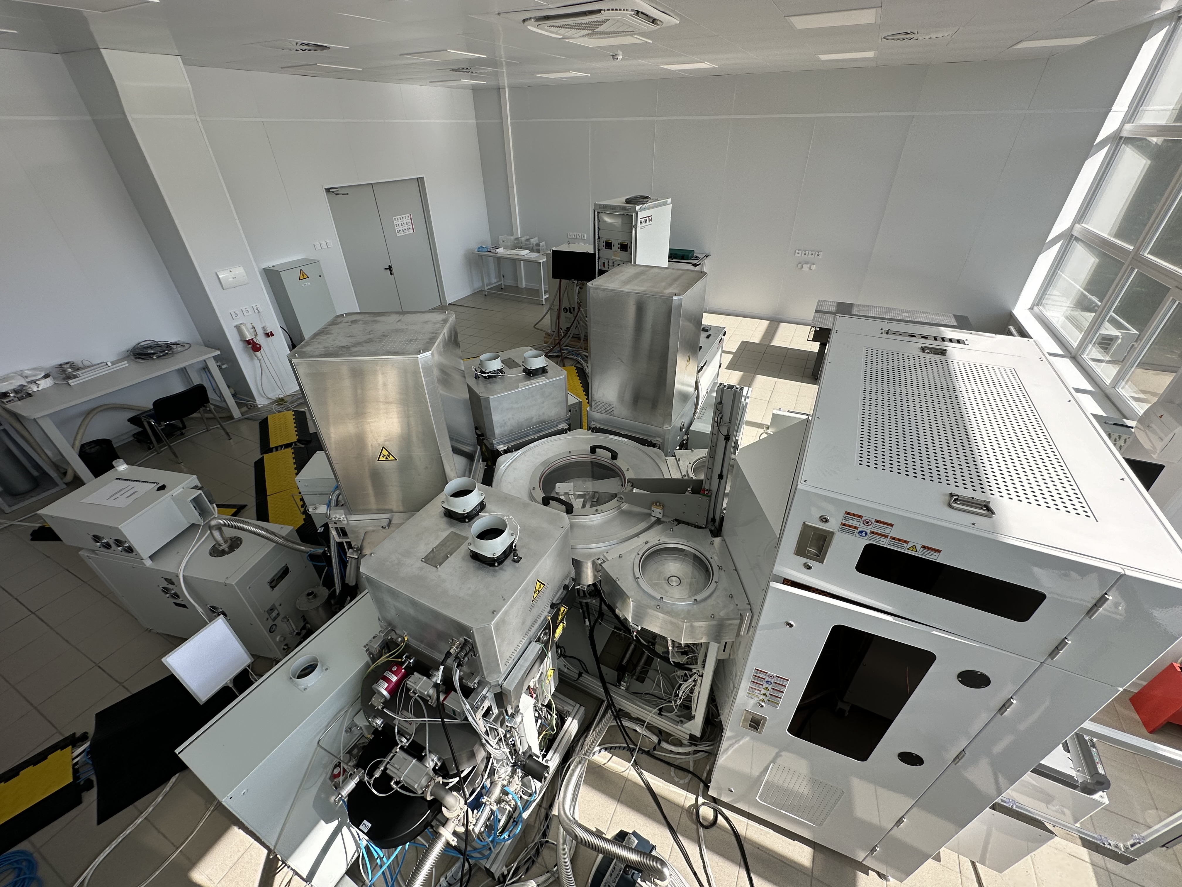
      The cluster installation is designed to carry out the processes of plasma chemical etching (ICP RIE) of metallization layers for the formation of metal wiring elements by plasma chemical etching of Al (aluminum) using a photoresistive mask on functional substrates.
      More
      Specifications:
      Possibility of integration into a clean room
      —
      Yes
      Wafer diameter
      —
      200mm
      Wafer loading
      —
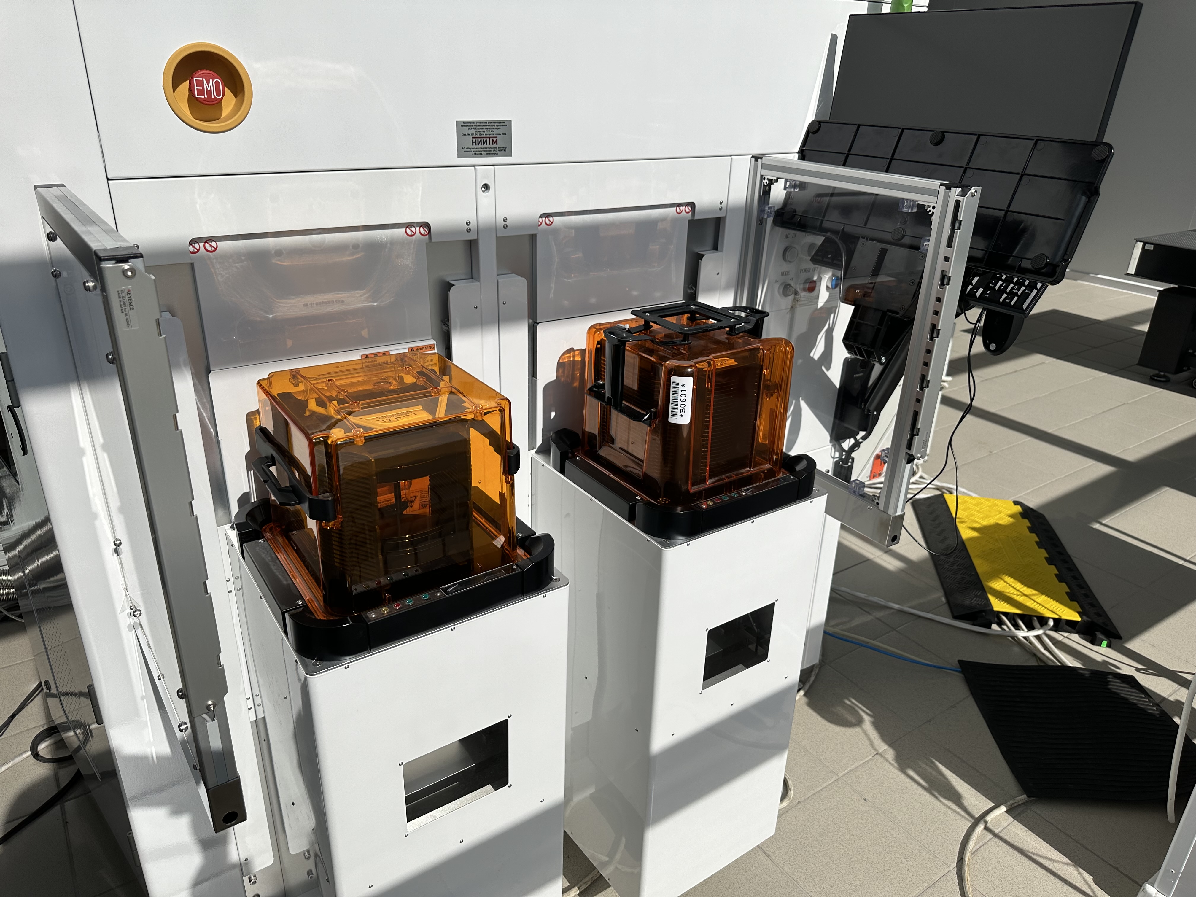
      SMIF container
      Цена действительна только для интернет-магазина и может отличаться от цен в розничных магазинах
      Cluster PCE Al
      Contact us
      Ask a question
      Additional options are possible
      • Description
      • Additionally

      Technological characteristics:

      • The size of the processed substrates, up to Ø mm – 200;
      • The number of simultaneously loaded substrates is 1;
      • The maximum thickness of the etched metal (Al), up to microns – 5;
      • Etching rate of silicon, polysilicon, A/min 9000
      • Selectivity of FR/AL* – 1: 2;

      • Uneven etching, %:
        1. on the plate – ±5
        2. from plate to plate** – ±2.5
        3. from reactor to reactor** – ±4
      • Photoresist removal rate at 270℃, up to microns/min – 3.5
      • Operating pressure range for Al modules, Pa – 1-10;
      • Operating pressure range for FR removal modules , Pa – 200-400;

      Energy supply:

      • Electric power consumption, kW, not more than – 85;
      • Voltage and frequency of the supply network, V, Hz – 380, 50;
      • Compressed air, overpressure, MPa – (0.3 - 0.4)
      • Overall dimensions of the installation (WxDxH) mm – 5000*4500*2200
      • Installation weight, not more than kg – 3500

      Warranty and post-warranty service;

      The possibility of upgrading and reconfiguring equipment to meet customer requirements.

      Back
      Company
      About the company
      Development history
      Equipment
      Classification of equipment
      Cluster equipment
      New developments
      Catalog search
      Contacts
      +7(495)229-75-01
      +7(499)735-13-69 - Marketing department
      Contact us
      E-mail
      marketing@niitm.ru
      Address
      Zelenograd, Panfilovsky Prospekt, 10
      Operating mode
      Mon - Thu: 08:30 - 17:30
      Fri: 08:30 - 16:15
      marketing@niitm.ru
      Zelenograd, Panfilovsky Prospekt, 10
      © 2026 niitm.ru
      Privacy policy