CLUSTER PolySi RIE
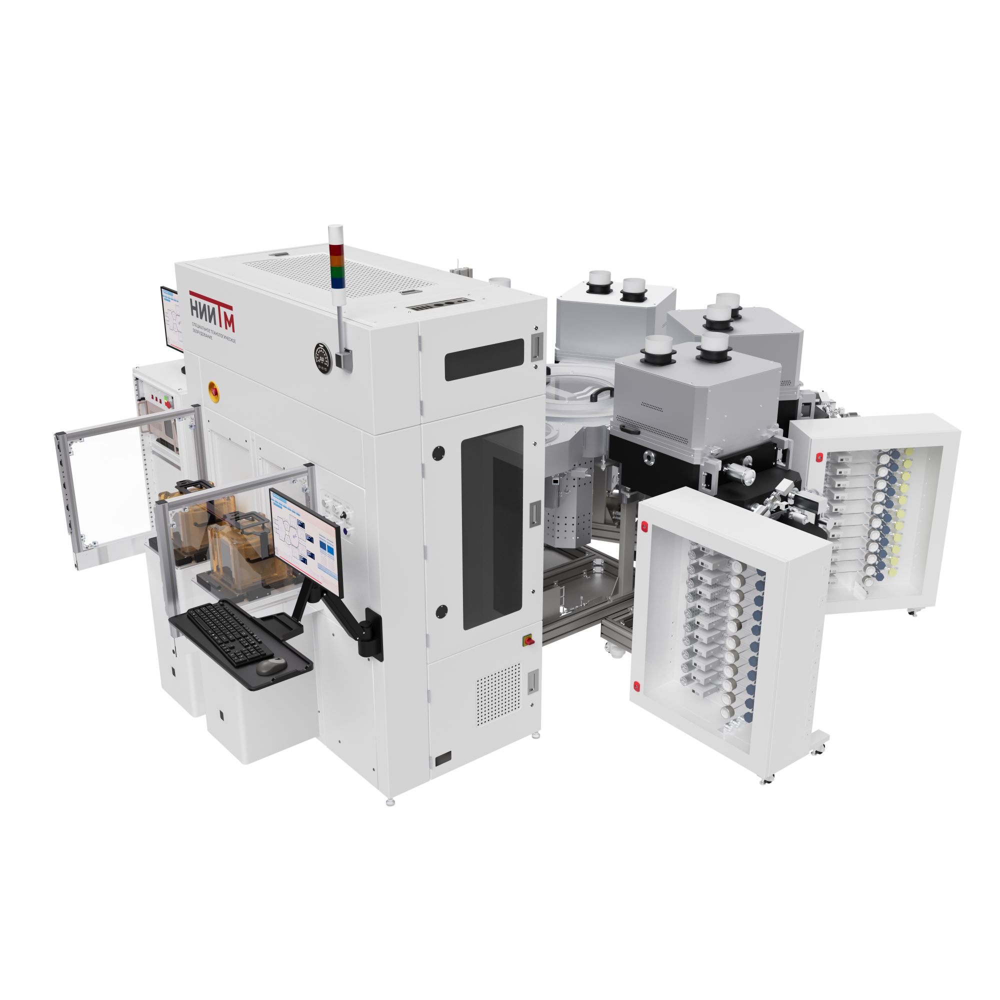
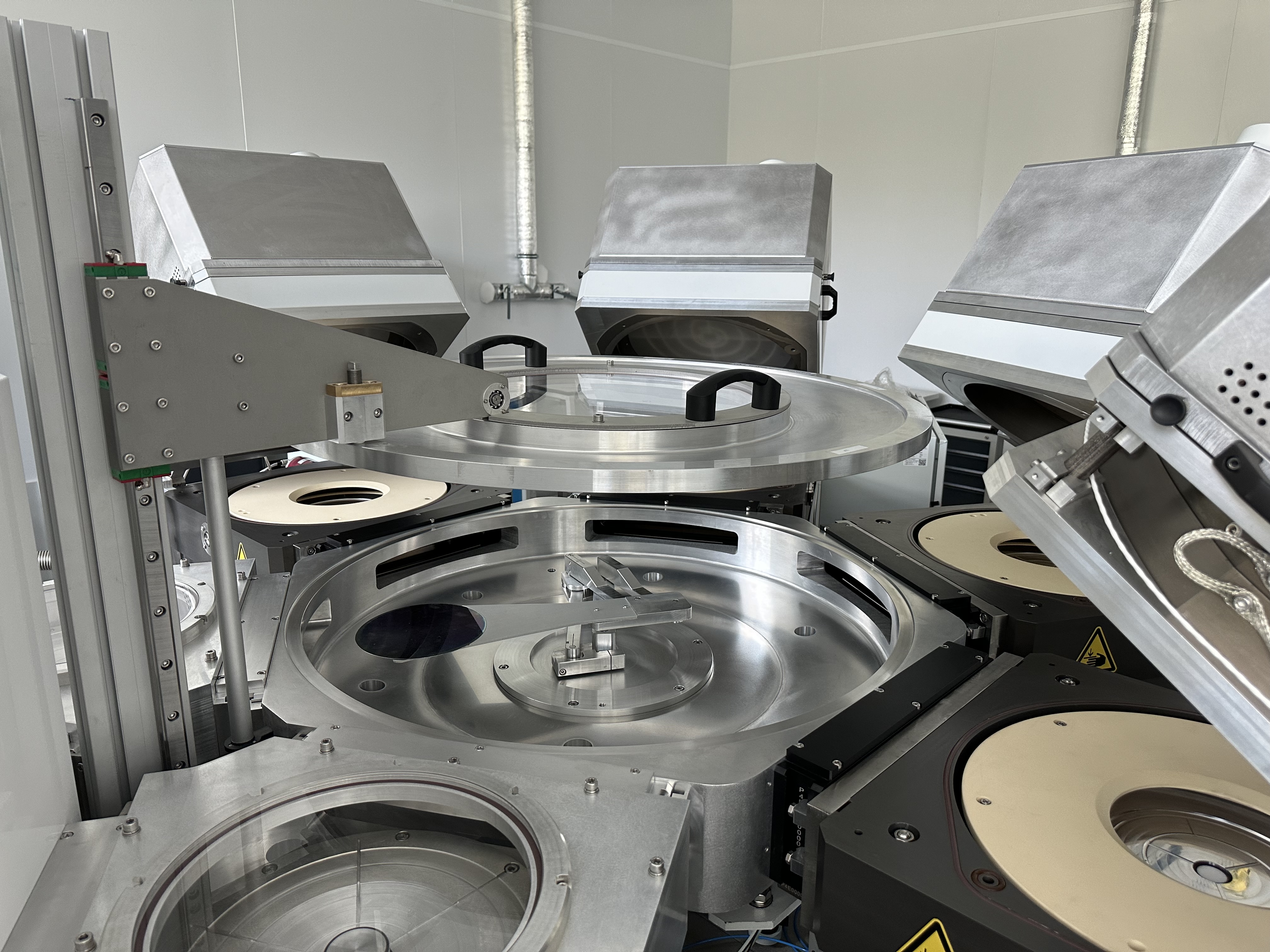
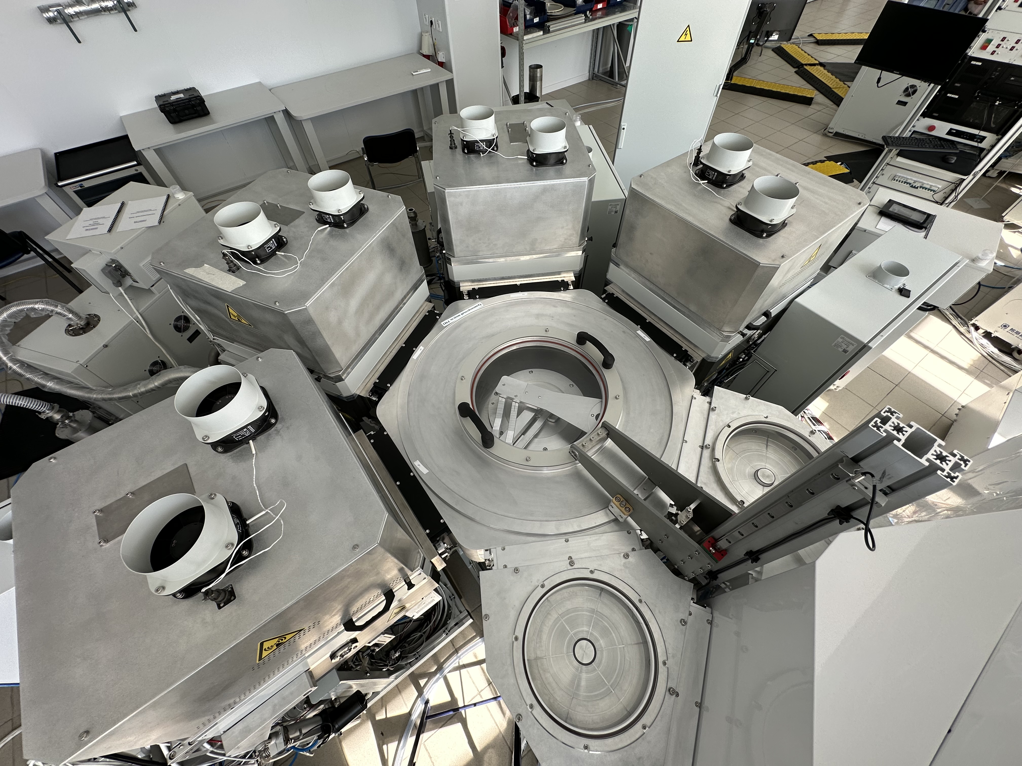
3D


The cluster system is designed to carry out the processes of plasma chemical etching of polysilicon to form circuit elements (gates of various types, slit insulation) by plasma chemical etching of silicon using a photoresistive mask and a rigid mask on functional substrates.
Specifications:
Possibility of integration into a clean room
—
Yes
Wafer diameter
—
200mm, 300mm
Wafer loading
—
SMIF container
Цена действительна только для интернет-магазина и может отличаться от цен в розничных магазинах
CLUSTER PolySi RIE
Loading...
Specifications:
- The size of the processed substrates, up to Ø mm 200;
- The number of simultaneously loaded substrates 1;
- Etching rate of silicon, polysilicon, A/min > 2000;
-
Requirements for etching processes, microns:
- maximum thickness of poly etchback 1
- maximum etching depth STI 1
- maximum etching depth of trench contacts 1
- the maximum etching thickness of the polysilicon gate 0.5
-
Selectivity:
- etching of silicon and polysilicon with respect to photoresist 15:1 at the main etching stage
- etching of silicon and polysilicon with respect to silicon oxide 100:1 at the stage of overdrawing
-
Uneven etching, %:
- along the plate ±3
- from plate to plate ±2.5
- from reactor to reactor ±4
- Operating pressure range, Pa 1-10;
Energy supply:
- Electric power consumption, kW, not more than 85;
- Voltage and frequency of the supply network, V, Hz 380, 50;
- Compressed air, overpressure, MPa 0.3 - 0.4
- Overall dimensions of the installation (WxDxH) mm 5000*4500*2200
- Installation weight, not more than kg 3500
Warranty and post-warranty service;
The possibility of upgrading and reconfiguring equipment to meet customer requirements.